9 Stone Feature Wall Ideas to Completely Transform Your Living Room
Your living room is the heart of your home—a place for relaxation, entertainment, and making memories. But if it's feeling a little stale, how can you make a powerful change? The answer lies in adding a natural stone feature wall.
A stone accent wall brings unparalleled texture, depth, and character to any space. It’s a timeless investment that elevates your interior from ordinary to extraordinary. To get your creative juices flowing, we've gathered 15 inspiring natural stone feature wall ideas that will make your living room the talk of the town.
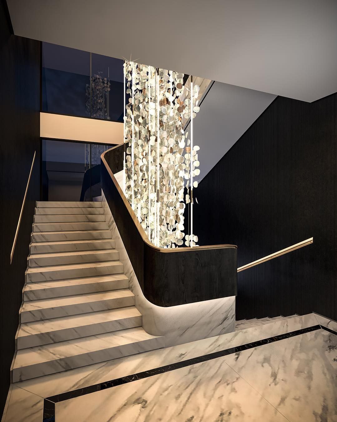
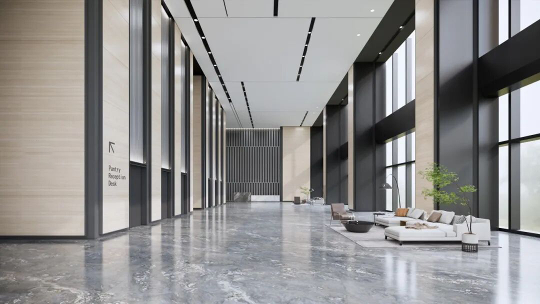
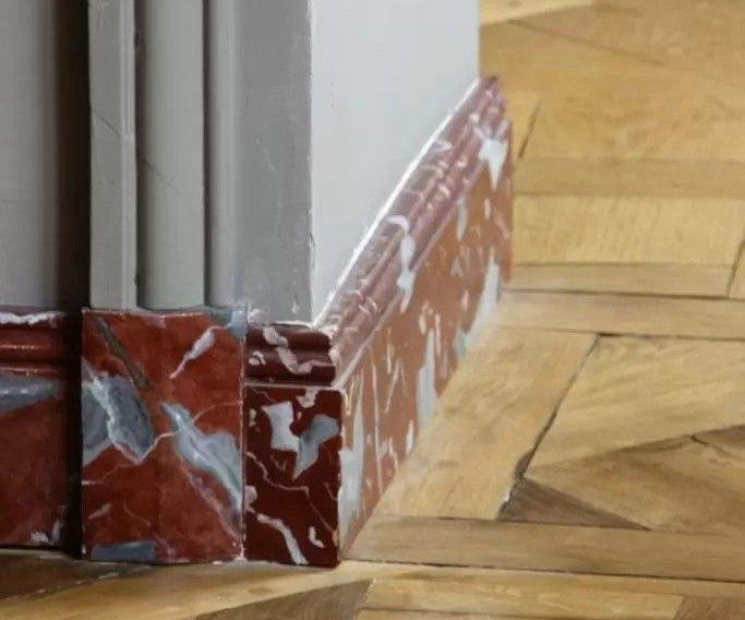
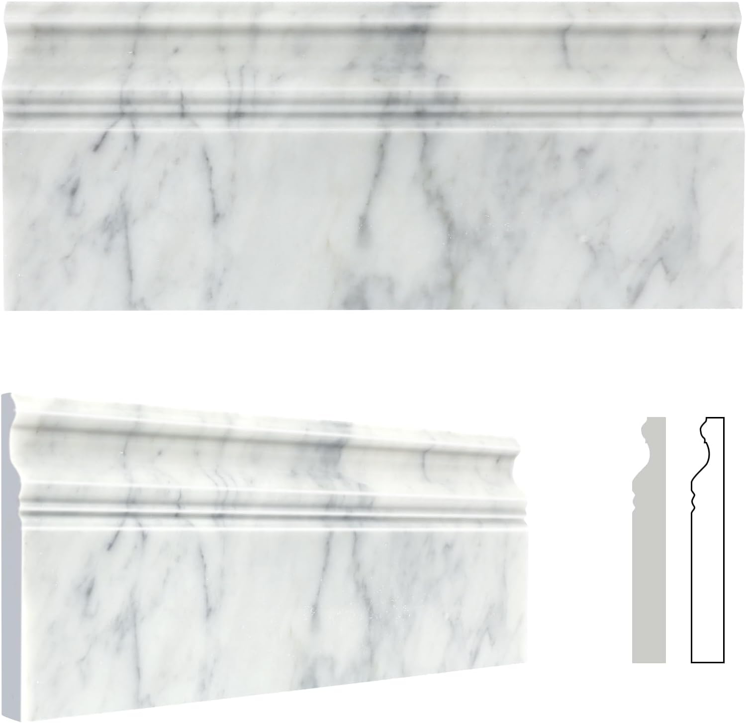
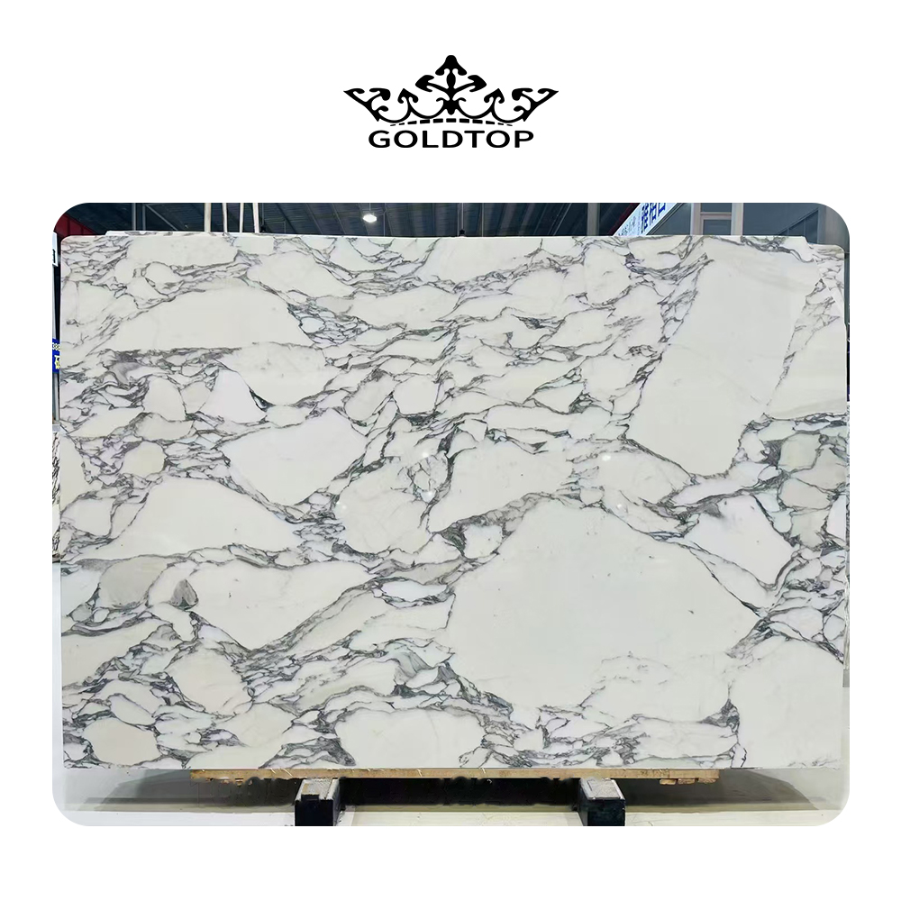
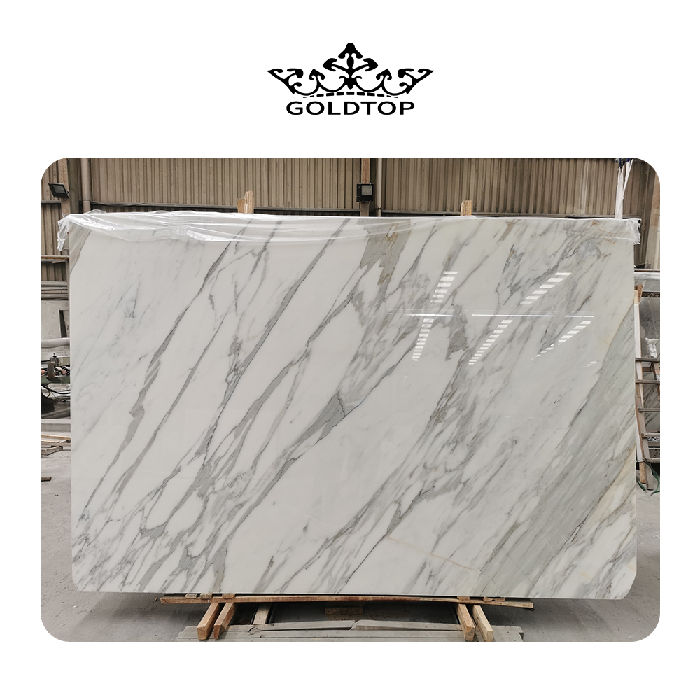
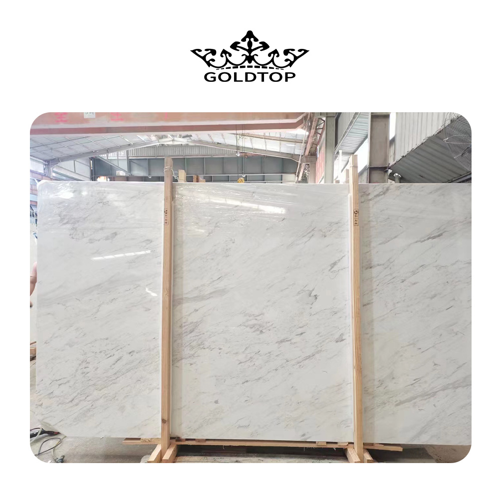
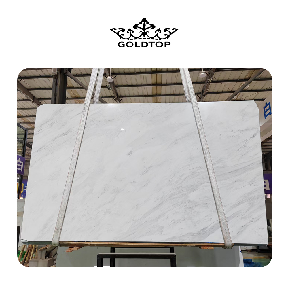
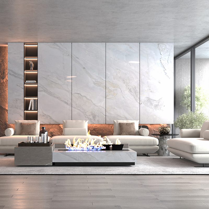
1. The Classic Marble Elegance
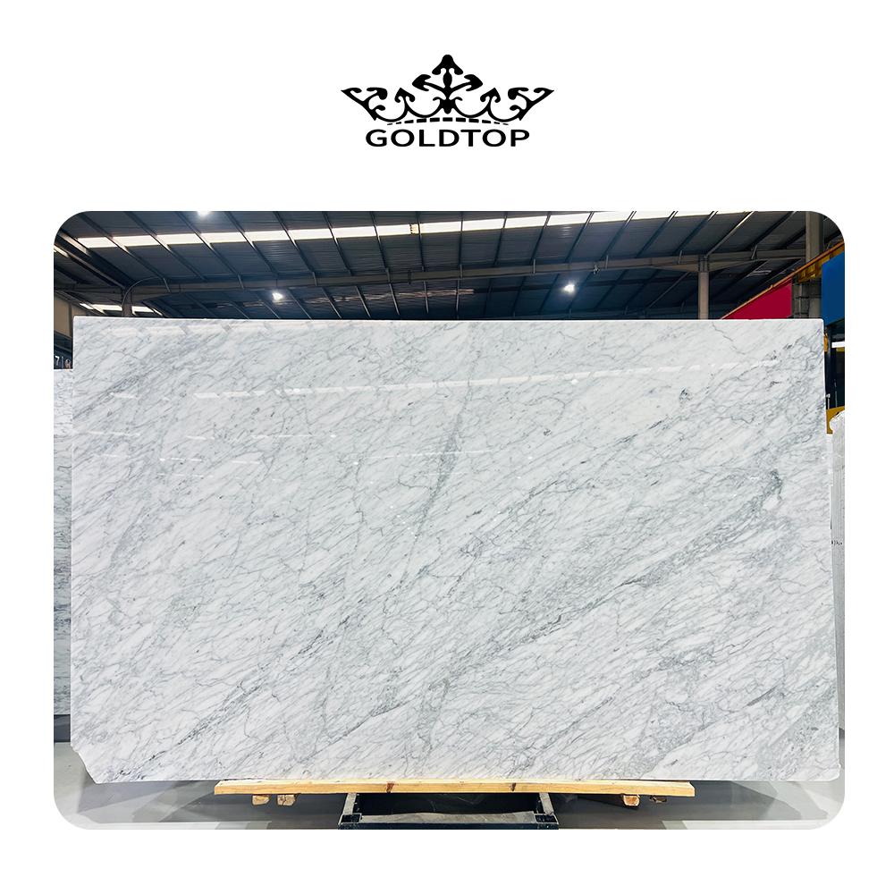
Nothing says luxury like a polished marble feature wall. Choose a statuary white or sky white slab with soft, flowing veins. This look creates a bright, sophisticated, and airy atmosphere, perfect for a minimalist or modern luxury home.
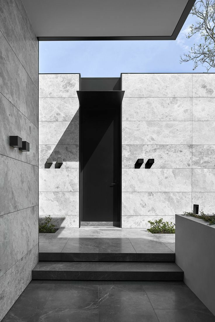
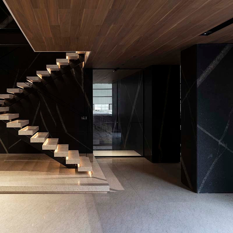
2. Industrial Chic with Honed Granite
Move beyond the polished look with honed granite. Its matte finish and granular texture are perfect for an industrial or urban loft style. The subdued tones and lack of shine emphasize the raw, natural beauty of the stone.
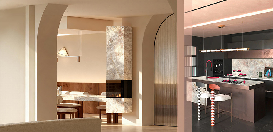
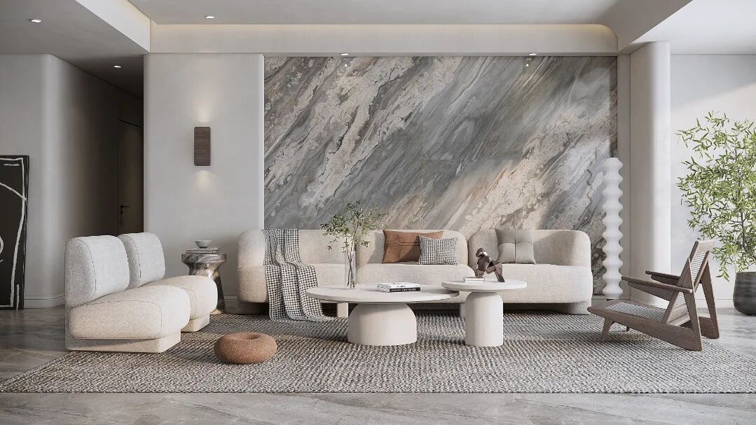
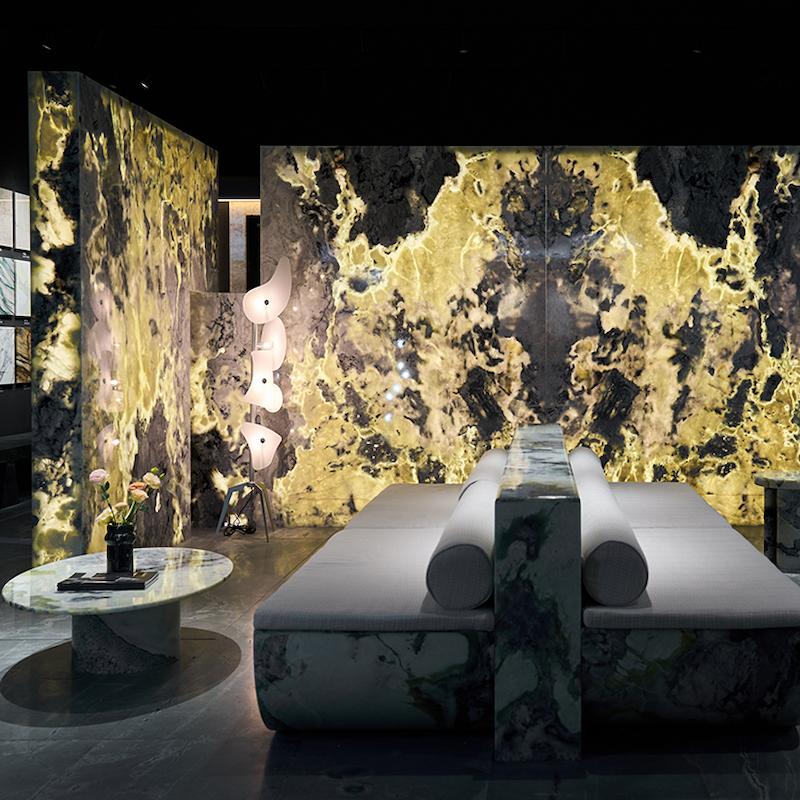
3. Dreamy Technology: The Backlit Marble Feature Wall
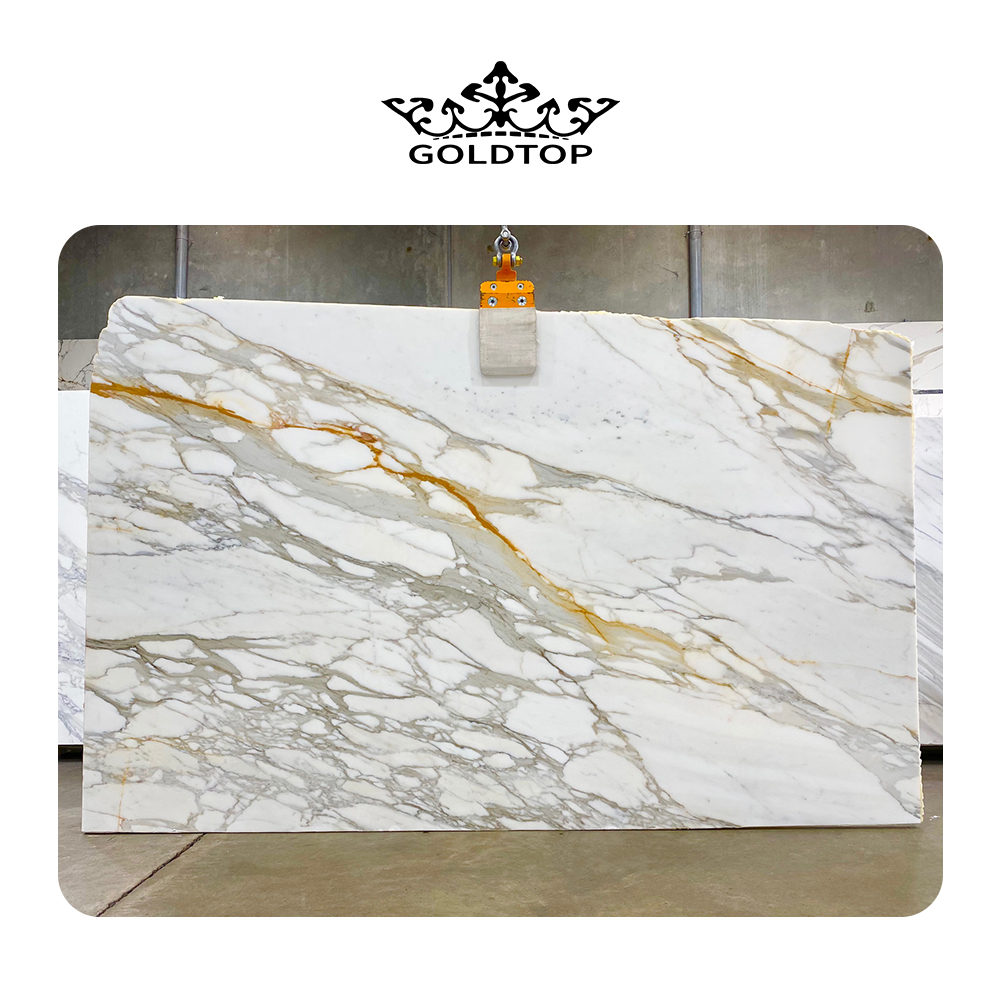
Combine the beauty of nature with modern technology to create a truly unique visual focus. A backlit marble feature wall is achieved by placing LED strip lights behind translucent marble (such as some types of Statuario or Onyx) or ultra-thin stone composite panels.
When the lights are on, the rays penetrate the stone and diffuse softly, dramatically highlighting and elevating its warm hues and natural veins. You can adjust the color (often warm white for a cozy feel) and brightness of the light to suit different scenes and moods. This design is not only the pinnacle of luxury but also imbues the space with a sense of futurism and an art-gallery-like ambiance, making it the undeniable soul of the room.
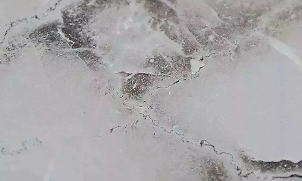
4. Subtle Sophistication with Limestone
If you prefer a softer, more neutral palette, limestone is your perfect choice. Its earthy tones and subtle, uniform texture provide a serene and elegant backdrop that doesn’t overwhelm the space.
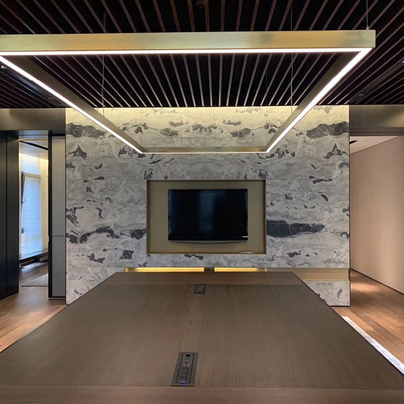
5.The Sleek TV Wall Unit
Integrate your entertainment center seamlessly by building your TV console and shelving directly into a stone feature wall. This creates a clean, unified, and high-end custom look.
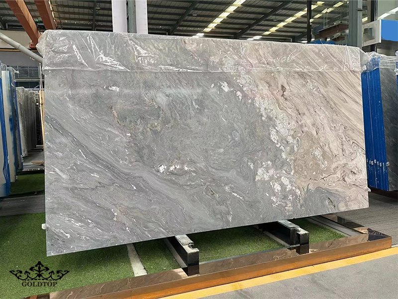
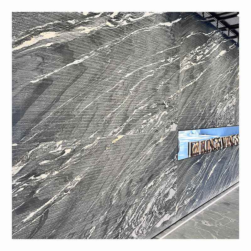
6.Advanced Texture: Special Finishes on Grey Stone
Go beyond traditional polished and honed finishes to explore the revolutionary textures that special processing brings to grey stone. Through techniques like flaming, Corteccia, or brushing, grey stone (such as granite, basalt, or certain marbles) develops a micro-rough surface that begs to be touched.
It creates a low-key, restrained, yet deeply rich minimalist and high-end aesthetic, perfectly suited for modern wabi-sabi, minimalist, or premium commercial spaces.
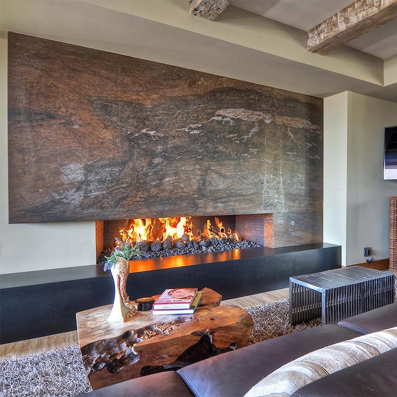
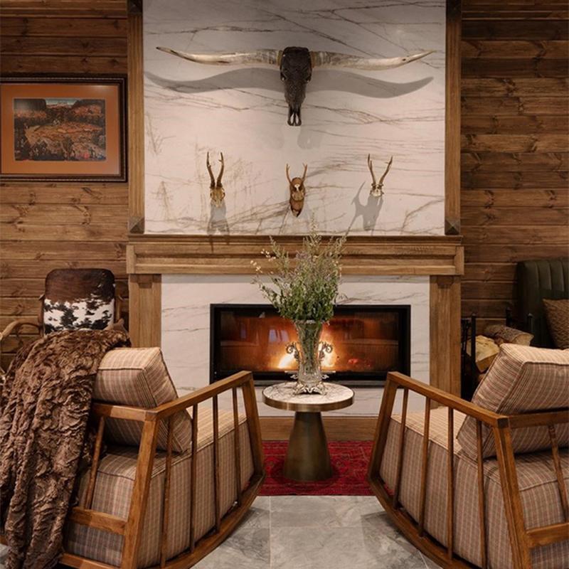
7.The Cozy Fireplace Surround
Focus your design around the hearth. A natural stone fireplace surround, whether in rugged granite or elegant marble, instantly becomes the warm, inviting centerpiece of your living room.
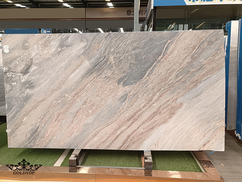
8.Quartzite for Durability and Beauty
For those who love the look of marble but need superior durability, quartzite is the hero. It offers similar beautiful veining but is much more resistant to scratches and etching, making it perfect for a busy family home.
9.A Sliver of Stone as an Accent
You don't need a full wall to make an impact. Use a thin, vertical strip of a striking stone to frame a doorway, a fireplace, or one section of the wall. It's a modern and cost-effective way to incorporate natural stone.
Ready to Bring Your Vision to Life?
As you can see, the possibilities with natural stone are truly endless. It’s more than just a building material—it’s a way to inject personality, luxury, and timeless beauty into your home.
At Kings-wing, we specialize in helping homeowners and designers find the perfect stone for their vision. Browse our gallery of premium natural stones or contact our experts today for a free consultation. Let's transform your living room together!
? Contact Us Today!
? Browse Our Stone Collection